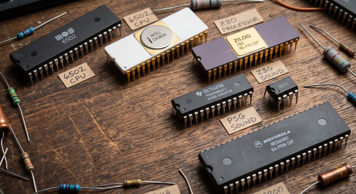
The Interactive IC Pinout & Datasheet Quick-Finder launched with 26 chips. As of today it holds 56. Thirty new parts went in, and they fill the gaps that actually matter for repair work: the CPUs, the support chips that sit around them, the sound and video chips, and — finally — memory.
Every pinout was checked against a manufacturer datasheet or an equivalent primary source before it went in. I will come back to why that matters, because the process caught me being wrong three times.
What went in
- CPUs (8): the 6502, the C64's 6510, the C16/Plus-4 8501, the C128's 8502, Motorola's 6809, Intel's 8080A and 8085A, and the still-in-production W65C02S.
- Support chips (7): the 6522 VIA, the 6526 CIA, the 6821 PIA, the 6850 ACIA, Intel's 8255 PPI and 8253 PIT, and the 82S100 — the C64 PLA.
- Sound and video (8): the VIC-II, the 8580 SID, the VIC-20's 6560, the 6845 CRTC, the AY-3-8910 and its Yamaha cousin the YM2149, TI's SN76489, and the TMS9918A video chip.
- Memory (5) — a brand new category: the 2114 SRAM, the 4116 and 4164 DRAMs, the 6264 SRAM and the 2764 EPROM.
- Analogue and interface (2): the MAX232 and the LM358.
The swap that destroys chips: 4116 versus 4164
If you take one thing from this update, take this one. The 4116 and the 4164 are both 16-pin dynamic RAMs that look identical on the board. They are not interchangeable, and fitting the wrong one kills it.
The 4116 needs three supply rails. Pin 1 is −5 V substrate bias, pin 8 is +12 V, pin 9 is +5 V and pin 16 is ground. The 4164 dropped all that for a single rail — so on a 4164, pin 1 is a no-connect, pin 8 is the +5 V supply, and pin 9 is address line A7.
Put a 4164 in a 4116 socket and you are feeding +12 V into a 5 V supply pin and driving a 5 V rail into an address input. It will not survive the power-up. Going the other way it simply will not work. Adapter boards exist for exactly this reason, and both pages now carry the four-pin comparison side by side.
While on the 4164: its VCC is pin 8 and its ground is pin 16, which is the exact reverse of nearly every other 16-pin DIP you will ever handle. Put 5 V on pin 16 out of habit and the chip is gone.
Where the power pins are not
A theme ran through this batch. Plenty of 1980s chips do not put the supply at the diagonal corners, and reaching for pin 40 out of muscle memory is expensive:
- The 6522, 6526, 6821 and 6845 all put VCC on pin 20. Pin 40 on a 6522 is CA1 — an input-only control line. Five volts there damages the chip.
- The 6850 ACIA puts ground on pin 1 and VCC on pin 12 — both on the same side of the package.
- The 8255 has ground on pin 7 and VCC on pin 26. Neither is at a corner.
- The 8080A needs three rails: −5 V on pin 11, +5 V on pin 20 and +12 V on pin 28 — and pin 28 sits in the middle of the address bus, between A2 and A3. The −5 V also has to come up before the +12 V and go down after it, or you can destroy the chip. A missing −5 V rail gives flaky, heat-dependent nonsense rather than a clean failure, which makes it a classic misdiagnosis.
- The VIC-II has three supply pins, and pin 13 is +12 V on a 6567/6569 but +5 V on an 8562/8565. Fit the HMOS part where the NMOS one belongs and you put 12 V into a 5 V chip. C64 boards 250407 and earlier are the 12 V ones; 250425, 250466 and 250469 are 5 V. Check the board revision before you order the chip.
The W65C02S is not a drop-in 6502
You will see this claimed constantly. It is not true, and the reason is genuinely dangerous.
On an NMOS 6502, pin 1 is ground. On WDC's W65C02S, pin 1 is VPB — Vector Pull, an output. On a board that hardwires pin 1 to the ground plane, that output tries to pull high into a copper plane every time it is released. The plane wins, a lot of current goes through the output transistor, and the chip degrades or dies.
WDC's own application note AN-002 tells you to bend pin 1 outward before fitting the chip to an Apple-1 or Apple II. Pin 5 (Memory Lock, also an output) gets the same treatment, and pin 36 (Bus Enable, an input) must be tied high. Worth knowing: the Rockwell R65C02 and GTE G65SC02 in 40-pin DIP are pin compatible — it is specifically the WDC part that adds the vector-pull output. That is why some people report a clean swap and others cook a chip.
Two chips that number their bits backwards
TI inherited MSB-first bit numbering from the TMS9900, and it shows up in two parts here.
On the SN76489, D0 is the most significant bit of the byte you write. Published pinouts for this chip openly contradict each other as a result — some say pin 1 is D5, we say pin 1 is D2 — because various authors quietly renumbered the bus to match modern convention. I followed TI's own Application Manual and documented the conflict on the page rather than picking a side and hoping. One source I found contradicts itself: its diagram says pin 1 is D5 while its own wiring table says D2. Check which convention any pinout you find is using before you wire from it.
The TMS9918A does the same thing across all three of its buses — CD0, AD0 and RD0 are all most-significant bits. It also has three separate 8-bit buses using 24 of its 40 pins: one to the CPU, one carrying VRAM addresses and write data out, and a third bringing VRAM read data back in. And pin 34 is a mild hazard: it is an active-low reset, but above +9 V it becomes a sync input for external video.
Port C, and other things in no sensible order
The 8255 deserves a special mention. Its Port C nibbles run in opposite directions: the upper nibble descends PC7, PC6, PC5, PC4 across pins 10 to 13, then the lower nibble ascends PC0, PC1, PC2, PC3 across pins 14 to 17. The sequence down that side of the chip is 7, 6, 5, 4, 0, 1, 2, 3. Port A is split across the package and descends; Port B is a clean ascending run. Three ports, three different conventions. Its RESET on pin 35 is also active high, unlike almost everything else of the era — if it is stuck high, every port stays in input mode and your outputs do nothing.
The 8253 timer is no better: its three counters appear in three different pin orders. Counter 0 is clock, out, gate. Counter 1 is out, gate, clock. Counter 2 is gate, out, clock. There is no pattern and nothing to infer from one counter to the next.
A few more quick ones. The 8501 has a seven-pin I/O port that runs P7, P6, then straight to P4 — there is no P5 pin, whatever Wikipedia's prose says. The 2114 numbers its data pins from one: DQ1 to DQ4, with no DQ0. The AY-3-8910 puts audio channel B on pin 3, channel A on pin 4, and channel C right across the package on pin 38. The LM358's two halves are mirrored, so the inputs swap round between them. And the 6845 has two address buses running in opposite directions, which is why a reversed row address gives you scan lines in the wrong order and looks exactly like a dead character ROM.
On the happier side, the 2764 EPROM and 6264 SRAM differ in only four pins — pin 1, 20, 26 and 27. Every address line, every data line, ground, VCC and /OE are identical. That is the JEDEC 28-pin byte-wide standard, and it is why ROM-to-RAM adapters are so simple.
Why I check everything twice
I know these chips. I have had most of them in a socket at some point. And while building this batch, cross-checking against datasheets caught me being wrong three times:
- On the 6510 I had the I/O port and the data bus in the wrong pin positions entirely.
- On the 6821 I had two of the three chip selects the wrong way round.
- On the 6845 I had the whole second half of the package wrong.
All three would have rendered as perfectly tidy, confident-looking diagrams. That is the problem with pinout data — a wrong pin number does not look wrong. So nothing here comes from memory, and I verified all 970 pins in this batch against the source tables before publishing.
What I left out, and why
The Amiga's Fat Agnus is still absent, for the same reason as at launch: Commodore's Hardware Reference Manual and the community wikis disagree about where its data bus starts, and an 84-pin pinout off by two bit positions is worse than no page.
The AY-3-8912 — the 28-pin single-port version in the Amstrad CPC — is mentioned on the AY-3-8910 page but has no diagram. I could only find one source for it, and it marked a bus-control pin active-low where nothing else does. One shaky source is not enough.
And there is still no PLCC or QFP part. The renderer handles PLCC and the geometry is tested, but I have not yet found a square-package pinout I can verify to the same standard. It will go in when I can.
Also fixed
A few things that were quietly broken. The 68000 page's datasheet link had been returning a 403 since launch — fixed. Eleven pages that had placeholder reference links now point at real datasheet PDFs, and all 58 datasheet links across the library have been checked as live. Nine meta descriptions were running long enough for Google to truncate them and have been tightened.
What's next
The library is built to grow — a new chip is one data file, and it appears in the search, the category filters and the sitemap automatically. Next on the bench: the Z80 support family (CTC, PIO, SIO), the FDC controllers, more of the Amiga custom chips if I can settle their pinouts, and a PLCC part to finally exercise that side of the renderer.
If there is a chip you keep having to look up, tell me and it goes to the front of the queue. Have a dig around the IC Pinout & Datasheet Quick-Finder and let me know what needs fixing.
Comments (0)
No comments yet. Be the first to comment on Smiggy's article!
Leave a Comment