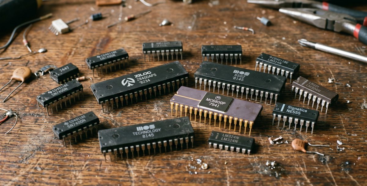
There is a new tool on the bench: an Interactive IC Pinout & Datasheet Quick-Finder. Point it at a chip and it draws the package, colour-codes every pin by what the pin actually does, and tells you the direction, the logic levels and the function when you click one. Twenty-six chips are in the library to start with, and every pinout has been checked against the manufacturer's datasheet rather than copied off a forum post.
The reason I built it is simple. Most of my repair time goes on the same question: what is this pin supposed to be doing, and what should I see on it? A pinout on its own does not answer that. Knowing pin 7 is called /MREQ is not much use unless you also know it is an output, that it is active low, and that it should be pulsing rather than sitting still.
Colour-coded pins, and a legend that isolates them
Every pin is grouped and coloured by function: power, ground, clock and timing, address bus, data bus, control, general I/O, analogue, and no-connect. On a 40-pin CPU that turns an intimidating wall of labels into something you can read at a glance — the address bus is one colour, the data bus another, and the handful of control lines you actually care about stand out.
The legend doubles as a filter. Click "Address Bus" and everything else dims, so you can see just the bus you are tracing. Click it again to bring the rest back. Active-low signals are marked with a leading slash — /RESET, /OE, /MREQ — so you are not left guessing which pins are asserted low.
Hover or click any pin and you get its number, name, function group, signal direction (input, output, bidirectional, tri-state or open-drain), the expected logic levels or voltage, and a plain-English description of what it does. It is keyboard navigable too: tab into the diagram and use the arrow keys to walk the pins. On a phone the package scales and scrolls, with zoom buttons rather than relying on pinch-to-zoom behaving itself.
A page for every chip
Each chip also has its own page — the Z80, the SID 6581, the 74LS245 and so on. Those pages carry the diagram pre-loaded, a summary spec block (technology, supply voltage, clock speed, propagation delay, logic thresholds), the full pin table in plain HTML so it works with JavaScript switched off, notes on where the part actually turns up and how it fails, direct links to the official datasheet PDF, and links to related chips in the same family.
Six pinout traps I ran into building it
Transcribing a few dozen datasheets back to back is a good way to be reminded how many parts look interchangeable and are not. These are the ones worth committing to memory:
- The CD4011 is not a drop-in for the 74LS00. Both are quad 2-input NAND gates. The 74LS00 puts its gate outputs on pins 3, 6, 8 and 11; the CD4011 puts them on 3, 4, 10 and 11. Swap one for the other without rewiring and you are driving gate outputs onto pins the board is driving as inputs.
- The 74LS02 puts its outputs first. Unlike its own NAND sibling, the quad NOR has the output on the first pin of each group — outputs on 1, 4, 10 and 13. And the CMOS quad NOR, the CD4001, follows the CD4011 layout instead, so the TTL and CMOS versions of the same function do not match each other either.
- The CD4049 hides its supply pin. VDD is on pin 1, not the top-right corner where every other 14- and 16-pin part in the library puts it. VSS is on pin 8, and pins 13 and 16 are no-connects — so pin 16, the supply pin on most 16-pin chips, is connected to nothing at all here.
- Z80 pin 1 is A11, not A0. The address bus is split across the package: A11 to A15 at one end, A0 to A10 at the other, with A0 on pin 30. Assuming pin 1 is the bottom of the address bus is an easy and expensive mistake.
- The 74LS244 interleaves its two nibbles. The 74LS245 is a clean split — A1 to A8 down one side, B8 to B1 back up the other. The 74LS244 alternates the inputs and outputs of its two 4-bit groups down the package instead, so you cannot pattern-match one from the other.
- The 74LS373 and 74LS374 occupy identical pin positions and differ only in what pin 11 does: a level-sensitive latch enable on the 373, an edge-triggered clock on the 374. Substituting one for the other gives you a circuit that almost works, which is the worst kind of fault to chase.
Two more for the counter enthusiasts: the CD4017 and CD4040 both scatter their outputs around the package in no useful order — the CD4017 has Q0 on pin 3, Q1 on pin 2 and Q5 on pin 1 — and the 68000 has two separate VCC pins (14 and 49) and two separate grounds (16 and 53), so one good continuity check does not prove the rail.
What's in the library so far
- 74-series logic (14): 74LS00, 02, 04, 08, 14, 32, 74, 86, 138, 139, 244, 245, 373 and 374 — the gates, decoders, buffers and latches that make up most of the glue logic in an 8-bit machine.
- 4000-series CMOS (8): CD4001, 4011, 4013, 4017, 4040, 4049, 4066 and 4093.
- CPUs (2): the Zilog Z80 and the Motorola 68000, the latter in its 64-pin DIP form.
- Sound (1): the MOS 6581 SID, including the detail that its +12 V analogue supply on pin 28 becomes +9 V on the 8580.
- Analogue (1): the NE555, which links across to the existing 555 timer calculator.
Why there's no Fat Agnus yet
I wanted the Amiga's 8372A Agnus in the first batch, as the 84-pin PLCC case. It is not there, and that is deliberate. Commodore's own Hardware Reference Manual lists its pins 1 to 14 as RD15 down to RD2, with RD0 on pin 84. Amigawiki and Wikipedia both list the same pins as RD13 down to RD0. Those cannot both be right, and an 84-pin pinout with the data bus off by two bit positions is worse than no page at all. It goes in when I can settle it against a board schematic, not before.
What's coming next
The library is built to grow — adding a chip is one data file, so new parts appear in the search, the sitemap and the category filters automatically. Next on the list are the rest of the CPUs (6502, 6510, 8501, W65C02S, 6809, 8080A and 8085), the support chips that sit around them (6522 VIA, 6526 CIA, 6821 PIA, 6845 CRTC, 6850 ACIA, 8255 PPI, 8253 PIT and the C64 PLA), more sound and video (8580, VIC-II, AY-3-8910, SN76489, TMS9918A, YM2149), and the memory parts that fail most often — 2114, 4116, 4164, 6264 and the 2764 EPROM.
If there is a chip you keep having to look up, tell me and I will push it up the queue. Have a poke around the IC Pinout & Datasheet Quick-Finder and let me know what needs fixing.

Comments (0)
No comments yet. Be the first to comment on Smiggy's article!
Leave a Comment